
Electronics manufacturing has always evolved quickly, but the pace of change in PCB assembly is becoming especially intense as products become smaller, smarter, more connected, and more specialized. In 2026, printed circuit board assembly is no longer just about placing components accurately on a board; it is about building reliable, data-driven, highly customized electronic systems at scale. From artificial intelligence on the factory floor to advanced packaging, sustainability pressures, and resilient supply chains, the industry is entering a new phase where flexibility and precision matter as much as speed.
TLDR: PCB assembly in 2026 is being shaped by automation, artificial intelligence, miniaturization, sustainable manufacturing, and stronger supply chain strategies. Manufacturers are investing in smarter inspection systems, digital twins, advanced materials, and flexible production lines to meet demand for complex electronics. The result is a faster, more adaptive, and more quality-focused assembly process that supports industries ranging from medical devices and electric vehicles to aerospace and consumer technology.
From Manual Processes to Intelligent Manufacturing
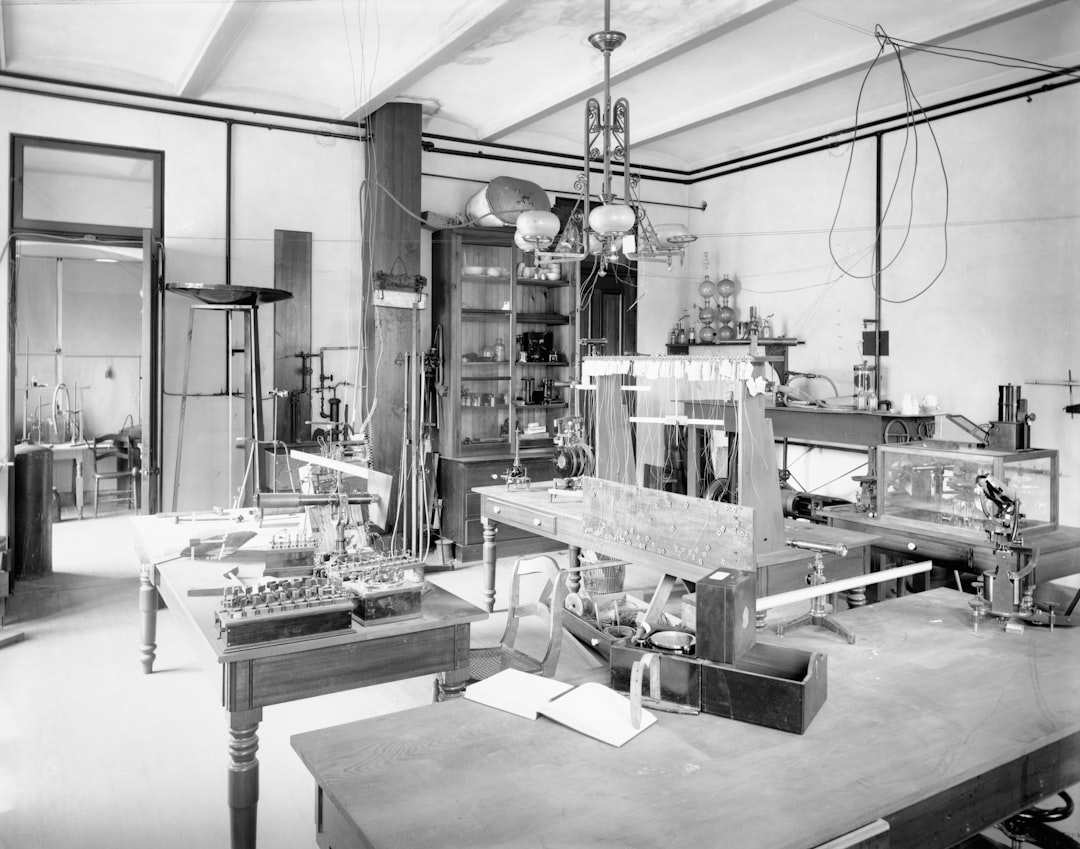
The evolution of PCB assembly has been a story of increasing precision. Decades ago, many assembly steps depended heavily on manual labor, through-hole components, and relatively simple board layouts. As surface mount technology became dominant, manufacturers gained the ability to place tiny components at high speed, dramatically improving production efficiency and enabling more compact electronic devices.
By 2026, however, PCB assembly has moved beyond traditional automation. The most competitive facilities are becoming intelligent manufacturing environments, where machines do not simply follow programmed instructions but continuously collect data, adjust processes, and identify potential defects before they affect final products.
This shift is especially important because today’s circuit boards are more complex than ever. Modern PCBs often include high-density interconnects, fine-pitch components, embedded modules, radio frequency sections, power electronics, sensors, and advanced thermal management features. Producing these boards requires a level of control that older assembly methods cannot consistently deliver.
Artificial Intelligence Becomes a Core Production Tool
One of the most important trends shaping PCB assembly in 2026 is the rise of artificial intelligence. AI is no longer a futuristic concept reserved for experimental factories. It is increasingly used in everyday production to improve inspection, scheduling, process control, and predictive maintenance.
In automated optical inspection systems, AI can help distinguish between true defects and harmless variations. Traditional inspection systems often rely on rigid rule sets, which can lead to false positives or missed issues when board designs vary. AI-based inspection tools can learn from large image datasets, making them better at identifying solder bridges, insufficient solder, tombstoning, component misalignment, polarity errors, and surface contamination.
AI is also changing how manufacturers maintain equipment. Instead of waiting for a pick-and-place machine, reflow oven, or stencil printer to fail, manufacturers can monitor vibration, temperature, cycle counts, and performance patterns. Predictive maintenance systems can then recommend service before a breakdown occurs. This reduces downtime and improves overall production reliability.
The biggest value of AI is not that it replaces skilled engineers, but that it gives them better visibility into processes that were once difficult to measure in real time.
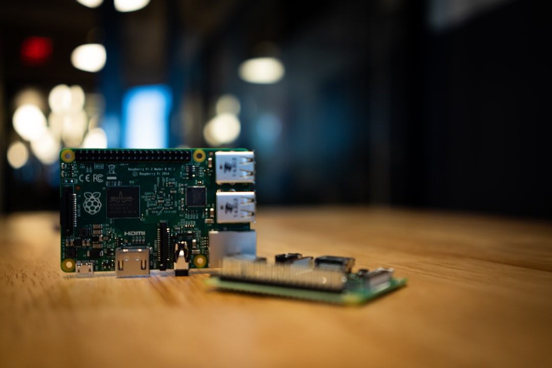
Miniaturization and High-Density Design Continue to Accelerate
Consumer devices, wearables, medical implants, automotive sensors, and industrial Internet of Things products are all pushing PCB assembly toward smaller, denser, and more capable designs. In 2026, manufacturers are increasingly working with components that are difficult to see clearly without magnification, including tiny passive components, chip-scale packages, micro BGAs, and advanced system-in-package modules.
This creates several assembly challenges:
- Tighter placement tolerances: Even slight misalignment can affect performance or reliability.
- More demanding solder paste printing: Smaller pads require highly controlled paste volume and stencil design.
- Greater inspection complexity: Hidden joints under BGAs and advanced packages require X-ray inspection and sophisticated analysis.
- Thermal management concerns: Dense boards generate heat in smaller spaces, requiring better materials and design strategies.
High-density assemblies are especially important in sectors such as aerospace, defense, telecommunications, and medical technology, where reliability must remain high despite compact form factors. As a result, PCB assemblers must combine precision equipment with deep process knowledge.
Advanced Packaging Blurs the Line Between PCB and Semiconductor Assembly
Another important development is the growing overlap between PCB assembly and semiconductor packaging. As electronic products demand higher speed, lower latency, and better energy efficiency, manufacturers are adopting advanced packaging approaches that place multiple functions closer together.
Technologies such as system in package, embedded components, chiplets, and heterogeneous integration are changing how engineers think about circuit architecture. Instead of relying solely on a traditional board populated with discrete components, designers may combine processors, memory, sensors, power management, and communication modules into compact integrated assemblies.
For PCB assemblers, this means new process requirements. Handling moisture-sensitive parts, controlling warpage, managing fine-pitch interconnects, and ensuring clean assembly environments are becoming increasingly important. The boundary between board assembly and microelectronics assembly is becoming less distinct, and manufacturers that can bridge both worlds are gaining a competitive advantage.

Automation Expands Beyond Component Placement
Pick-and-place automation has been standard in high-volume PCB assembly for many years, but in 2026 automation is extending across the entire production workflow. Facilities are investing in automated material handling, robotic soldering, automated conformal coating, selective soldering, depaneling, labeling, testing, and packaging.
This broader automation trend is driven by several factors. Labor shortages remain a challenge in many manufacturing regions, especially for highly skilled technical roles. At the same time, customers expect faster turnaround times and consistent quality. Automation helps manufacturers meet these expectations while reducing manual handling, which can introduce defects or electrostatic discharge risks.
However, modern automation is not only about replacing repetitive work. It is also about traceability. Automated systems can record which machine placed each component, which solder paste batch was used, what reflow profile was applied, and what inspection results were generated. This level of documentation is essential for industries such as automotive, aerospace, and medical electronics.
Digital Twins and Data Driven Process Control
In 2026, more PCB assembly companies are using digital twins to model and optimize production. A digital twin is a virtual representation of a product, process, or production line. In PCB assembly, it can be used to simulate material flow, identify bottlenecks, predict yield issues, and evaluate process changes before they are implemented on the factory floor.
For example, a manufacturer may use a digital model to test how a new board design will move through stencil printing, placement, reflow, inspection, and testing. If the simulation shows a risk of thermal imbalance during reflow, engineers can adjust the profile or recommend design changes before full production begins.
Data-driven process control also supports continuous improvement. Instead of reviewing quality issues after a batch is complete, engineers can monitor performance in near real time. If solder paste volume begins drifting out of specification, the system can alert operators immediately. This helps prevent small variations from becoming expensive production failures.
Sustainability Becomes a Manufacturing Priority
Sustainability is no longer a secondary concern in electronics manufacturing. Governments, customers, and investors are placing greater pressure on manufacturers to reduce waste, improve energy efficiency, and use safer materials. PCB assembly is affected by this trend at every stage, from material sourcing to end-of-life recycling.
Lead-free solder has already been widely adopted in many markets, but sustainability efforts now go further. Manufacturers are looking at lower-temperature soldering processes, energy-efficient reflow ovens, improved chemical management, recyclable packaging, and better waste reduction practices. Some facilities are also redesigning workflows to reduce scrap caused by setup errors, overproduction, or insufficient process control.
Sustainable PCB assembly is not just about environmental responsibility. It can also improve profitability. Reduced rework, lower energy consumption, and smarter inventory management all contribute to lower operating costs. In 2026, companies that can demonstrate sustainable practices are also more attractive to customers with strict environmental, social, and governance requirements.
Supply Chain Resilience Remains a Strategic Issue
The electronics industry has learned difficult lessons from component shortages, logistics disruptions, geopolitical tensions, and sudden demand swings. As a result, PCB assembly in 2026 is strongly influenced by the need for supply chain resilience.
Manufacturers are no longer relying as heavily on single-source suppliers or just-in-time inventory strategies without backup plans. Instead, they are building more flexible sourcing models, qualifying alternate components, maintaining closer communication with suppliers, and using software tools to monitor availability and risk.
Design teams are also becoming more supply-chain aware. Engineers increasingly consider component availability, lifecycle status, and second-source options during the design phase. This helps prevent costly redesigns later and makes production more stable.
Nearshoring and regional manufacturing are also gaining momentum. While global supply chains remain important, many companies want assembly partners closer to their final markets. This can reduce lead times, improve communication, and lower exposure to international shipping delays.
Testing and Inspection Grow More Sophisticated
As PCBs become more complex, testing is becoming more comprehensive. Basic visual inspection is no longer enough for many applications. In 2026, manufacturers commonly combine several inspection and testing methods to ensure reliability.
- Automated optical inspection: Used to identify visible placement and soldering defects.
- Automated X-ray inspection: Essential for hidden solder joints, BGAs, and dense assemblies.
- In-circuit testing: Verifies electrical characteristics and component-level performance.
- Functional testing: Confirms that the assembled board performs as intended in real operating conditions.
- Environmental testing: Used for products exposed to vibration, humidity, temperature extremes, or harsh conditions.
In high-reliability sectors, test data is increasingly linked to individual serial numbers, creating a detailed history for each PCB assembly. This traceability helps with compliance, warranty analysis, and long-term reliability studies.
Flexible Manufacturing Supports Customization
The old model of electronics production focused heavily on extremely high-volume runs of identical products. That model still exists, but demand is growing for lower-volume, high-mix manufacturing. Industrial equipment, specialized medical devices, robotics, aerospace systems, and custom IoT products often require smaller production batches with frequent design updates.
PCB assemblers are responding by making production lines more flexible. Faster machine setup, automated programming, modular fixtures, and digital work instructions allow manufacturers to switch between jobs more efficiently. This is particularly valuable for companies that need prototypes, pilot runs, and production builds from the same assembly partner.
In 2026, flexibility is a competitive advantage. The best PCB assembly providers are not only fast; they are adaptable.
The Growing Importance of Design for Manufacturability
As assembly complexity increases, design for manufacturability has become more important than ever. A board that looks good in design software may still create problems during assembly if pad sizes, component spacing, thermal reliefs, panelization, or solder mask clearances are not optimized.
Manufacturers are increasingly involved earlier in the product development process. By reviewing files before production, they can identify risks such as insufficient spacing, difficult solder joints, poor test access, or components that may be hard to source. Early collaboration reduces delays, improves yield, and lowers total product cost.
The most successful electronics companies treat PCB assembly as a design partner relationship rather than a final production step. This mindset helps turn complex concepts into reliable physical products.
What PCB Assembly Will Look Like Beyond 2026
Looking beyond 2026, PCB assembly will continue moving toward greater intelligence, precision, and integration. AI systems will become more capable, inspection will become more predictive, and production lines will become more autonomous. Materials will improve to support higher frequencies, better heat dissipation, and more demanding operating environments.
At the same time, the human role will remain essential. Engineers, technicians, and process specialists will be needed to interpret data, solve unusual problems, optimize designs, and make strategic manufacturing decisions. The future of PCB assembly is not a factory without people; it is a factory where people are supported by smarter tools.
Conclusion
The evolution of PCB assembly in 2026 reflects the broader transformation of electronics manufacturing. Products are becoming smaller, more powerful, and more connected, while customers expect faster delivery, higher reliability, and greater transparency. To meet these demands, manufacturers are embracing AI, automation, advanced inspection, digital twins, sustainable practices, and resilient supply chains.
For businesses developing electronic products, these trends create both opportunities and challenges. Choosing the right assembly partner now means looking beyond basic production capacity. It means evaluating technical expertise, process control, traceability, flexibility, and the ability to support innovation from prototype to full-scale manufacturing.
PCB assembly is no longer just a manufacturing step. It is a strategic foundation for modern electronics. In 2026, the companies that understand this shift will be best positioned to build the next generation of reliable, intelligent, and sustainable electronic products.